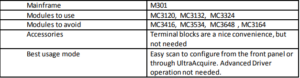
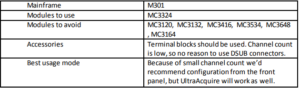
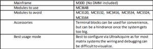
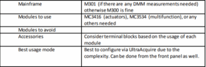
Overview
A Bode plot is a graph that maps the frequency response of the system. It was first introduced by Hendrik Wade Bode in 1940.
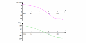
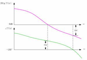
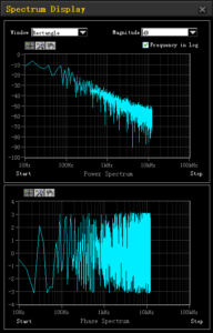
The Bode plot consists of the Bode magnitude plot and the Bode phase plot. Both the amplitude and phase graphs are plotted against the frequency. The horizontal axis is lgω (logarithmic scale to the base of 10), and the logarithmic scale is used. The vertical axis of the Bode magnitude plot is 20lg (dB), and the linear scale is used, with the unit in decibel (dB). The vertical axis of the Bode phase plot uses the linear scale, with the unit in degree (°). Usually, the Bode magnitude plot and the Bode phase plot are placed up and down, with the Bode magnitude plot at the top, with their respective vertical axis being aligned. This is convenient to observe the magnitude and phase value at the same frequency, as shown in the following figure.
The loop analysis test method is as follows: Inject a sine-wave signal with constantly changing frequencies into a switching power supply circuit as the interference signal, and then judge the ability of the circuit system in adjusting the interference signal at various frequencies according to its output.
This method is commonly used in the test for the switching power supply circuit. The measurement results of the changes in the gain and phase of the output voltage can be output to form a curve, which shows the changes of the injection signal along with the frequency variation. The Bode plot enables you to analyse the gain margin and phase margin of the switching power supply circuit to determine its stability.
Principle
The switching power supply is a typical feedback loop control system, and its feedback gain model is as follows:
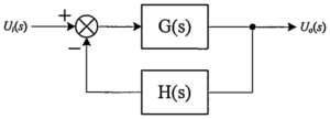
From the above formula, you can find out the cause for the instability of the closed-loop system: Given 1 + T(s) =0, the interference fluctuation of the system is infinite.
The instability arises from two aspects:
1) when the magnitude of the open-loop transfer function is:
2) when the phase of the open-loop transfer function is:
The above is the theoretical value. In fact, to maintain the stability of the circuit system, you need to spare a certain amount of margin. Here we introduce two important terms:
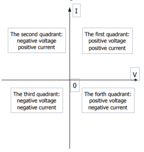
- PM: phase margin.
When the gain |T(s)| is 1, the phase <T(s) cannot be -180° . At this time, the distance between <T(s) and -180° is the phase margin. PM refers to the amount of phase, which can be increased or decreased without making the system unstable. The greater the PM, the greater the stability of the system, and the slower the system response.
- GM: gain margin.
When the phase <T(s)is -180°, the gain |T(s)| cannot be 1. At this time, the distance between |T(s)| and 1 is the gain margin. The gain margin is expressed in dB. If |T(s)| is greater than 1, then the gain margin is a positive value. If |T(s)| is smaller than 1, then the gain margin is a negative value. The positive gain margin indicates that the system is
stable, and the negative one indicates that the system is unstable.
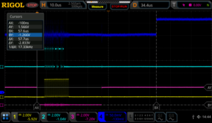
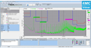
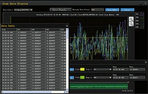
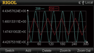
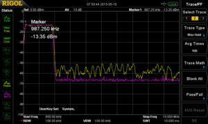
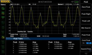
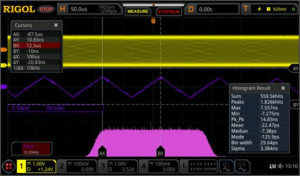
The following figure is the Bode plot. The curve in purple shows that the loop system gain varies with frequency. The curve in green indicates the variation of the loop system phase with frequency. In the figure, the frequency at which the GM is 0 dB is called “crossover frequency”.
The principle of the Bode plot is simple, and its demonstration is clear. It evaluates the stability of the closed-loop system with the open-loop gain of the system.
Loop Test Environment Setup
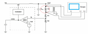
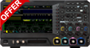
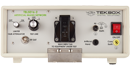
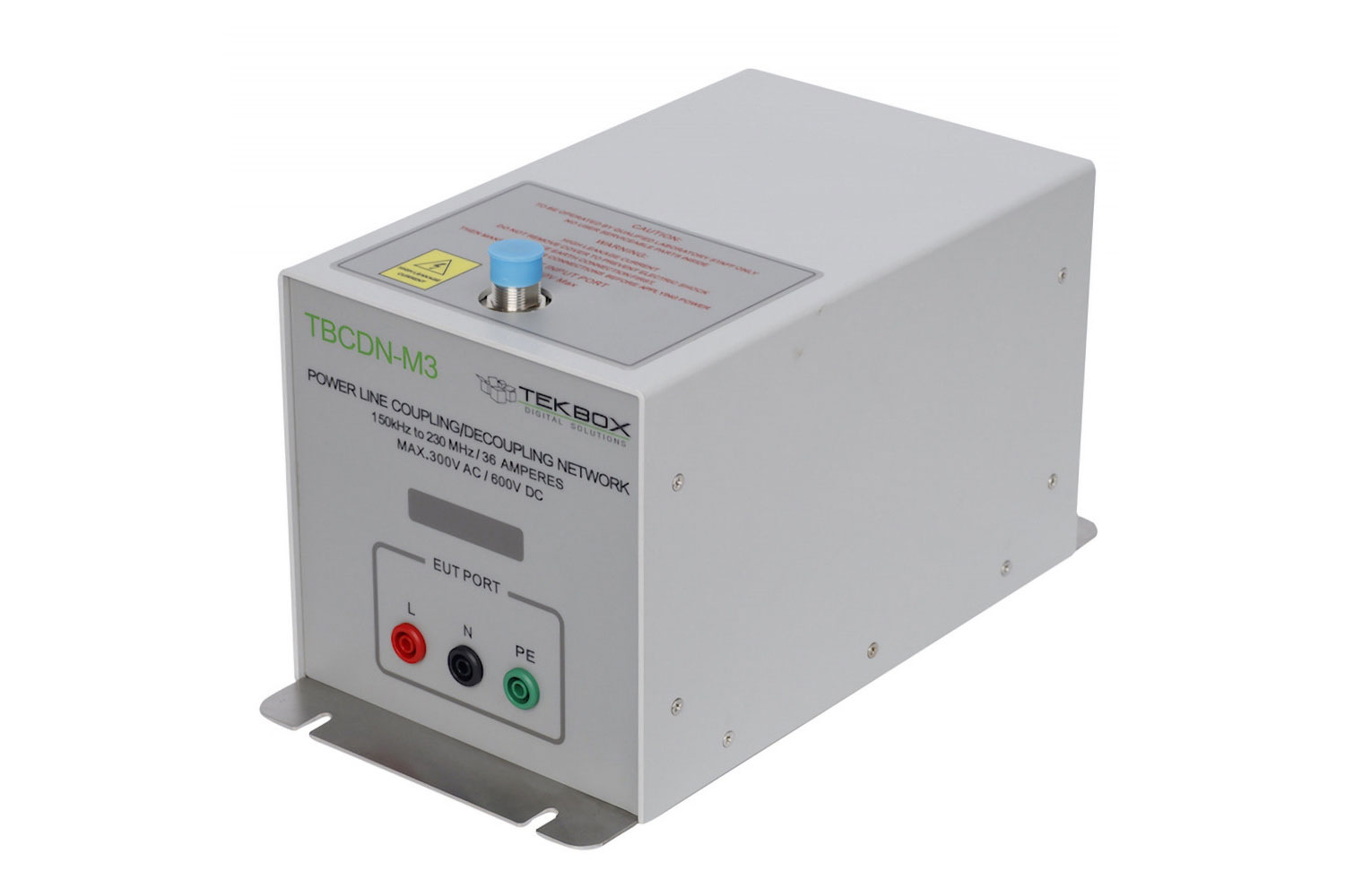
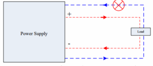
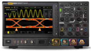
The following figure is the circuit topology diagram of the loop analysis test for the switching power supply by using RIGOL’s MSO5000 series digital oscilloscope. The loop test environment is set up as follows:
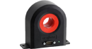
1. Connect a 5Ω injection resistor Rinj to the feedback circuit, as indicated by the red circle in the following figure.
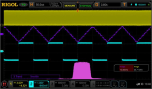
2. Connect the GI connector of the MSO5000 series digital oscilloscope to an isolated transformer. The swept sine-wave signal output from the oscilloscope’s built-in waveform generator is connected in parallel to the two ends of the injection resistor Rinj through the isolated transformer.
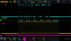
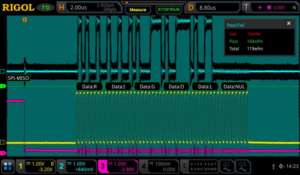
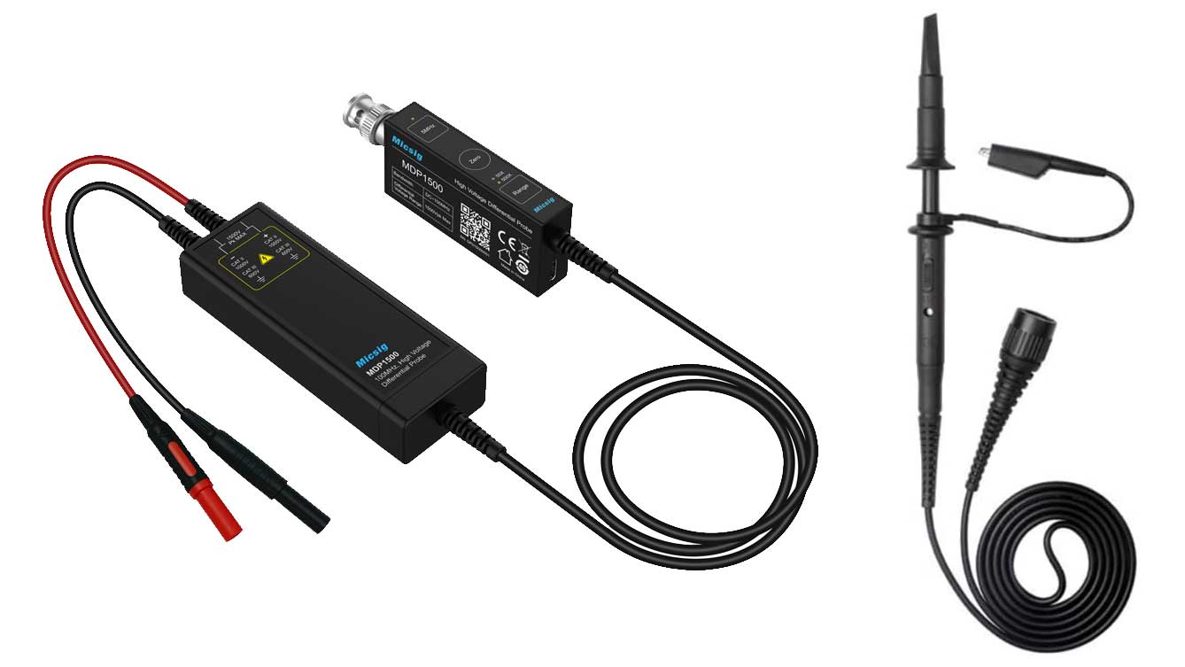
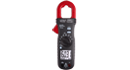
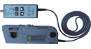
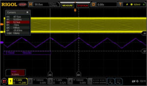
3. Use the probe that connects the two analogue channels of the MSO5000 series digital oscilloscope (e.g. RIGOL’s PVP2350 probe) to measure the injection and output ends of the swept signal.
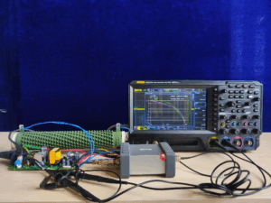
The following figure is the physical connection diagram of the test environment.
Operation Procedures
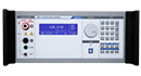
The following section introduces how to use RIGOL’s MSO5000 series digital oscilloscope to carry out the loop analysis. The operation procedures are shown in the figure below.
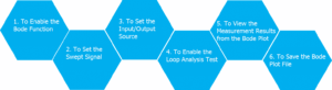
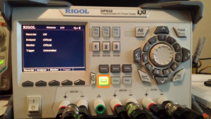
Step 1 To Enable the Bode Plot Function
You can also enable the touch screen and then tap the function navigation icon at the lower-left corner of the screen to open the function navigation. Then, tap the “Bode” icon to open the “Bode” setting menu.
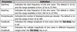
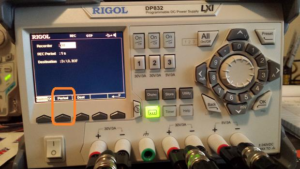
Step 2 To Set the Swept Signal
Press Amp/Freq Set. to enter the amplitude/frequency setting menu. Then the Bode Set window is displayed. You can tap the input field of various parameters on the touch screen to set the parameters by inputting values with the pop-up numeric keypad. Press Var.Amp. continuously to enable or disable the voltage amplitude of the swept signal in the different frequency ranges.
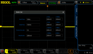
The definitions for the parameters on the screen are shown in the following table.
Note:
The set “StopFreq” must be greater than the “StartFreq”.
Press Sweep Type, and rotate the multifunction knob to select the desired sweep type, and then press down the knob to select it. You can also enable the touch screen to select it.
- Lin: the frequency of the swept sine wave varies linearly with the time.
- Log: the frequency of the swept sine wave varies logarithmically with the time.
Step 3 To Set the Input/Output Source
As shown in the circuit topology diagram in Loop Test Environment Setup, the input source acquires the injection signal through the analog channel of the oscilloscope, and the output source acquires the output signal of the device under test (DUT) through the analog channel of the oscilloscope. Set the output and input sources by the following operation methods.
Press In and rotate the multifunction knob to select the desired channel, and then press down the knob to select it. You can also enable the touch screen to select it.
Press Out and rotate the multifunction knob to select the desired channel, and then press down the knob to select it. You can also enable the touch screen to select it.
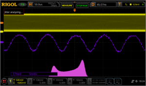
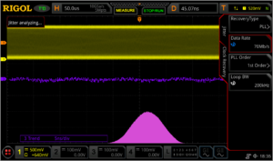
Step 4 To Enable the Loop Analysis Test
In the Bode setting, the initial running status shows “Start” under the Run Status key. Press this key, and then the Bode Wave window is displayed. In the window, you can see that a Bode plot is drawing. At this time, tap the “Bode Wave” window, the Run Status menu is displayed. Under the menu, “Stop” is shown under the Run Status menu.
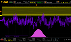
Step 5 To View the Measurement Results from the Bode Plot
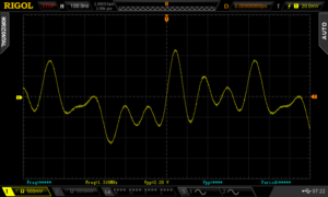
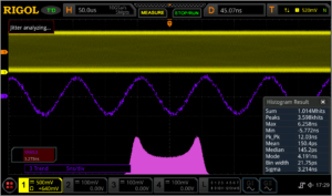
After the Bode plot has been completed drawing, the Run Status menu shows “Start” again. You can view the Bode plot in the Bode Wave window, as shown in the following figure.
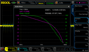
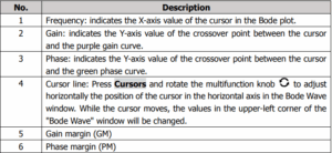
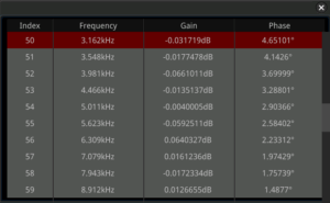
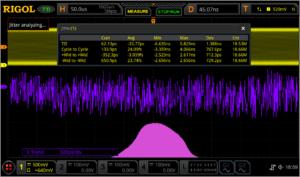
The following table lists the descriptions for the main elements in the Bode plot.
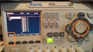
Press Disp Type and rotate the multifunction knob to select “Chart” as the display type of the Bode plot. The following table will be displayed, and you can view the parameters of the measurement results for loop analysis test.
Step 6 To Save the Bode Plot File
After the test has been completed, save the test results as a specified file type with a specified filename.
Press File Type to select the file type for saving the Bode plot. The available file types include “*.png”, “*.bmp”, “*.csv”, and “*.html”. When you select “*.png” or “*.bmp” as the file type, the Bode plot will be saved as a form of waveform. When you select “*.csv” or “*.html”, the Bode plot will be saved as a form of chart.
Press File Name, input the filename for the Bode plot in the pop-up numeric keypad.
Key Points in Operation
When performing the loop analysis test for the switching power supply, pay attention to the following points when injecting the test stimulus signal.
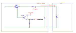
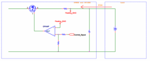
Selection of the Interference Signal Injection Location
We make use of feedback to inject the interference signal. Generally speaking, in the voltage-feedback switching power supply circuit, we usually put the injection resistor between the output voltage point and the voltage dividing resistor of the feedback loop. In the current-feedback switching power supply circuit, put the injection resistor behind the feedback circuit.
Selection of the Injection Resistor
When choosing the injection resistor, keep in mind that the injection resistor you select should not affect the system stability. As the voltage dividing resistor is generally a type that is at or above kΩ level, the impedance of the injection resistor that you select should be between 5Ω and 10Ω.
Selection of Voltage Amplitude of the Injected Interference Signal
You can attempt to try the amplitude of the injected signal from 1/20 to 1/5 of the output voltage.
If the voltage of the injected signal is too large, this will make the switching power supply be a nonlinear circuit, resulting in measurement distortion. If the voltage of the injected signal in the low frequency band is too small, it will cause a low signal-to-noise ratio and large interference.
Usually we tend to use a higher voltage amplitude when the injection signal frequency is low, and use a lower voltage amplitude when the injection signal frequency is higher. By selecting different voltage amplitudes in different frequency bands of the injection signal, we can obtain more accurate measurement results. MSO5000 series digital oscilloscope supports the swept signal with variable output frequencies. For details, refer to the function of the Var.Amp. key introduced in Step 2 To Set the Swept Signal.
Selection of the Frequency Band for the Injected Interference Signal
The frequency sweep range of the injection signal should be near the crossover frequency, which makes it easy to observe the phase margin and gain margin in the generated Bode plot. In general, the crossover frequency of the system is between 1/20 and 1/5 of the switching frequency, and the frequency band of the injection signal can be selected within this frequency range.
Experience
The switching power supply is a typical feedback control system, and it has two important indicators: system response and system stability. The system response refers to the speed required for the power supply to quickly adjust when the load changes or the input voltage changes. System stability is the ability of the system in suppressing the input interference signals of different frequencies.
The greater the phase margin, the slower the system response. The smaller the phase margin, the poorer the system stability. Similarly, if the crossing frequency is too high, the system stability will be affected; if it is too low, the system response will be slow. To balance the system response and stability, we share you the following experience:
● The crossing frequency is recommended to be 1/20 to 1/5 of the switching frequency.
● The phase margin should be greater than 45°. 45° to 80° is recommended.
● The gain margin is recommended to be greater than 10 dB.
Summary
RIGOL’s MSO5000 series digital oscilloscope can generate the swept signal of the specified range by controlling the built-in signal generator module and output the signal to the switching power supply to carry out loop analysis test. The Bode plot generated from the test can display the gain and phase variations of the system under different frequencies. From the plot, you can see the phase margin, gain margin, crossover frequency, and other important parameters. The Bode plot function is easy to operate, and engineers may find it convenient in analysing the circuit system stability.
Upgrade Method
Online Upgrade
After the oscilloscope is connected to network (if you do not have the access to the Internet, please ask the administrator to open the specified network authority) via the LAN interface, you can perform online upgrading for the system software.
1) Enable the touch screen and then tap the function navigation icon at the lower-left corner of the touch screen to enable the function navigation.
2) Tap the “Help” icon, and then the “Help” menu is displayed on the screen.
3) Press Online upgrade or enable the touch screen to tap “Online upgrade”, then a “System Update Information” window is displayed, requesting you whether to accept or cancel “RIGOL PRODUCT ONLINE UPGRADE SERVICE TERMS”. Tap “Accept” to start online upgrade. Tap “Cancel” to cancel the online upgrade.
For the local upgrade, please download the latest firmware from the following website and then perform the upgrade.
Products Mentioned In This Article:
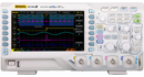
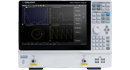
- MSO5000 Series please see HERE
- PVP2350 please see HERE


 FREE SHIPPING £75+
 CELEBRATING 50+ YEARS
 PRICE MATCH GUARANTEE


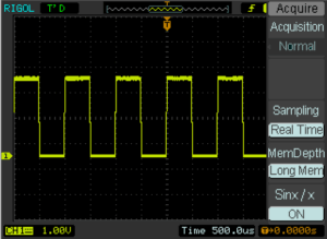 Sampling rate and Long Memory: