Free Shipping logo FREE SHIPPING £75+
50 years of Telonic Instruments Ltd logo CELEBRATING 50+ YEARS
Price Match logo PRICE MATCH GUARANTEE

Meeting Embedded Design Challenges with Mixed Signal Oscilloscopes

Posted on: June 16th, 2021 by Doug Lovell

Introduction

Embedded design and especially design work utilising low speed serial signalling is one of the fastest growing areas of digital electronics design. The need to communicate between modules, FPGAs, and processors within a wide array of consumer and industrial electronics is increasing at an astounding rate. Customised communication protocol and bus usage is critical to design efficiency and time to market, but comes with the risk of being sometimes difficult to analyse and debug. The most common sources and types of problems when using low speed serial data in an embedded application include timing, noise, signal quality, and data. We will recommend debug tips and features available in modern oscilloscopes that will make debugging these complex systems faster and easier.
Types of Errors
Timing
Timing is critical in any serial data system, but finding the system timing limitations related to components, transmission length, processing time, and other variables can be difficult. Let’s start with a simple 16 bit DAC circuit. First, make sure you understand the data and timing specifications for the protocol in use. Does it sample data right on the clock edge? How far off can the clock and data be when we still expect good data? In other words: do we have a clock sync error budget defined? Once we understand these timing requirements then we can experimentally verify both the Tx and Rx hardware subsystems. Now we can analyse the system level timing delays and the overall accuracy of the conversions because we can make direct measurements of both the logic and analogue channels in a time correlated fashion. We will also be able to simultaneously view the decoded bit patterns numerically on an oscilloscope that comes in well below your budget limits.
Here is a simple example of measuring a bit on channel 2 (blue) that is driving the DAC output that is creating the Sine wave on channel 1 (yellow).

Utilising parallel bus decoding (Figure 1) we can get a quick look at the transitions of this single line. But this doesn’t give us all the information we need since the DAC is utilising a number of data lines to set its output level. Getting more complete data requires a different approach. Let’s move all the DAC lines (Figure 2) over to the MSO’s digital inputs. Now we can see how the digital lines really coordinate with the DAC output. To investigate further we can simplify the decoding to show Hex values (Figure 3) and zoom in so we can view the decoded data.
Now we can use the zoom feature to clearly see the relationship between the bit and DAC transitions (Figure 4). For the zoom we have turned on analogue channel 2 in blue that is on the DAC clock. Zoomed in by a factor of 500x from 50 usec per division to 100 nsec per division allows us to see that the bit transitions are occurring 100 nsec before the clock transition. The clock transitions in under 5 nsec and the DAC output starts changing in sync with the clock. We can also utilise the scope cursors to make the timing in the transitions clearer and well defined (Figure 5).
Verifying timing in mixed signal systems can be made easier with the right tools. Select a modern scope with the correct set of channels and options to make sure you can easily view what you need on the display when you need it. From digital buses to processing delays, get the full picture of the device’s operation and delve into details as needed to verify timing issues on your device.

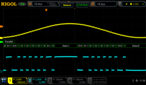
Figure 1: DAC output and input bit on a RIGOL MSO5354 Digital Oscilloscope

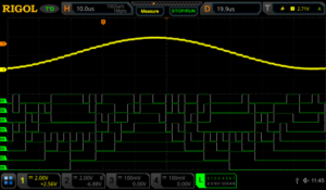
Figure 2: DAC output and 8 bit input bus on a RIGOL MSO5354 Digital Oscilloscope

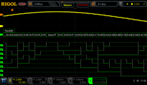
Figure 3: DAC output and 8 bit input bus with Hex decode on a RIGOL MSO5354 Digital Oscilloscope

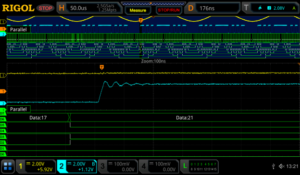
Figure 4: DAC output and 8 bit input bus zoomed in on a RIGOL MSO5354 Digital Oscilloscope


We can also trigger on the digital patterns instead of the analogue signal (Figure 6). Triggering on a digital pattern can be critical for debugging when there is a problem. There isn’t always a good way to track events from the analogue side of a system. When using a digital trigger method make sure to set the additional trigger parameters. These may include start bits or even address and data for some protocols. Even for a simple parallel bus like this you need to define and arrange the channels in the bus for the results to be easiest to interpret.
Accurate timing of Low Speed Serial signals is critical to system stability. Therefore, making sure your measurement tools are up to the task of precise and easy triggering, monitoring, and analysing of your waveforms is vital to improved R&D efficiency and ultimately time to market.

Noise

One of the most common issues in correct serial data measurements is the handling of system noise. Noise in these measurements can come from a number of sources including poor grounding, bandwidth issues, crosstalk, electromagnetic immunity (EMI) problems. Sometimes the problem is in the device, but improved probing and measurement techniques can also improve the results significantly without changing the device under test. A good first step is always to make sure we are using best measurement practices.
Here is a decoded I2C bus segment using a 5000 series oscilloscope (Figure 7). In the first example we have extremely poor grounding on our probes. Because the scope’s ground is tied directly to power ground signals that need to float or simply use a different or noisy ground plane can cause results like this. It is also possible for high current draw through ground in local power to create ground loops that can cause noise to be injected in your system. We solve these problems in order from easy to difficult. First, we can look at our probe connections. Normally, we would use the alligator clip ground strap that connects on the probe to make a ground connection. Assuming we are doing that correctly and still having a problem we may need to use the ground spring instead. The ground spring connects closer to the probe tip and significantly reduces the loop area of the connection. This can significantly improve noise and signal quality (Figure 8) especially for high speed signals or signals sensitive to capacitance or coupled voltages.

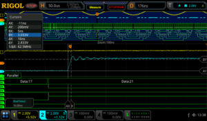
Figure 5: DAC output and 8 bit input bus zoomed in with cursors shown on a RIGOL MSO5354 Digital Oscilloscope

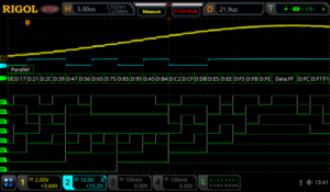
Figure 6: DAC output and 8 bit input bus triggered by a digital pattern on a RIGOL MSO5354 Digital Oscilloscope

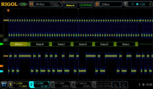
Figure 7: I2C clock and data with noise from poor grounding in a colour graded display using a RIGOL MSO5354 Digital Oscilloscope

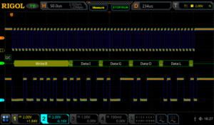
Figure 8: I2C clock and data with ground noise improved in a colour graded display using a RIGOL MSO5354 Digital Oscilloscope


All RIGOL probes come with both the standard ground strap and the ground spring for these types of measurements.
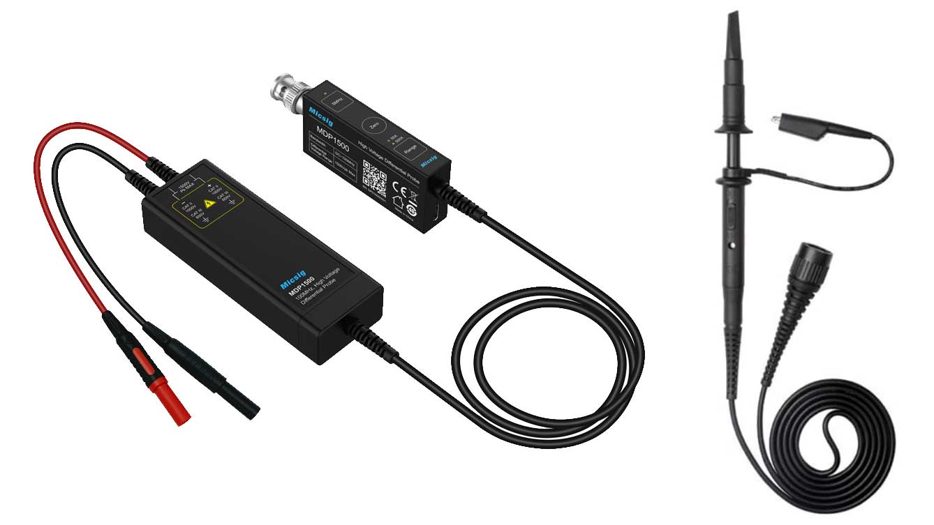
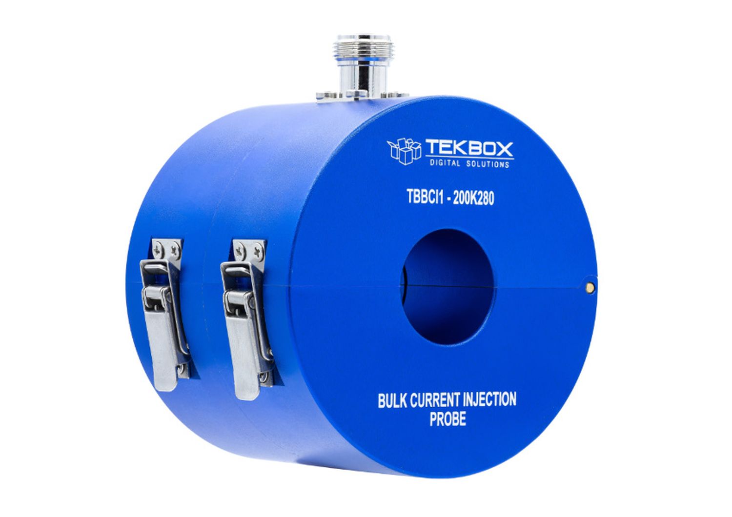
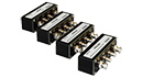
If ground noise is still an issue, try isolating your device from ground. The scope operates best grounded to AC power ground via the plug. If the rest of the device or system being tested can be isolated from ground this eliminates ground loops. If ground noise is still an issue you may consider a differential probe like the RP1100D (Figure 9) which enables measurements without reference to ground on the scope. Differential measurements may be the only way to clearly view some low speed serial data such as a LVDS bus (Low Voltage Differential Signalling). Buses like this purposely move the reference line to maximise bandwidth and increase communication distances, but it may require true differential probing or the use of multiple channels of your scope together to view the signal correctly. RIGOL has several different probe types for these measurements including the RP1000D series differential probes typically used for high voltage floating applications and the RP7150 1.5 GHz differential probe (Figure 10) for high speed data applications.

Now that we have improved our signal to noise ratio by decreasing noise injected from the ground, we can turn our attention to bandwidth filtering. High frequency noise can also enter your measurements via channel to channel cross talk or other high frequency sources nearby or within your

device. One way to address this is to utilise the channel bandwidth limits (Figure 11). Every RIGOL scope channel can limit the bandwidth to the ADC. A 20 MHz limit is pretty standard. Some scopes will have higher options as well.
Additionally, there are a few acquisition mode and triggering settings that can improve performance in the face of noise. Many trigger types have a menu item allowing you to turn on noise rejection for the triggering scheme. The 5000 series even includes HFR and LFR (high and low frequency rejection) as options in how to couple the signal triggered on. The 5000 series comes with High Res or High Resolution mode (Figure 12). This feature uses extra oversampling that is being done behind the scenes on many measurements to provide an average that results in less noise. This is best to use if you are able to set the sampling to take at least 200 samples per time division. This will average rather than reject high frequency signals, so be sure to understand your potential error sources and how they may interact with your measurement setup. Finally, the 5000 series scope also has an NRJ (noise reject) feature directly within the trigger menu. This removes noise that appears in bursts and can be set in time rather than frequency.
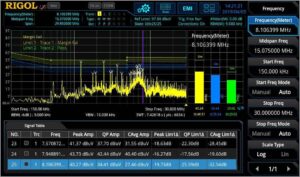
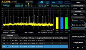
To further isolate and locate sources of noise within your system you may want to focus on EMC or EMI related issues. To further investigate these error sources please download the EMC Precompliance app note for use with the Rigol DSA815 Spectrum Analyser at https://www.rigolna.com/EMC

Noise is always a concern when working with low speed serial signals. By definition these signals continue to go to higher speeds, more advanced encoding, farther transmission distances, and lower voltage and power levels. All of these trends make hardware more susceptible to noise. Making careful measurements that limit or eliminate adding noise to our system then enables us to focus on noise in the system that may still cause long term design issues.

Figure 9: RP1100D 100 MHz Differential Probe

Figure 10: RP7150 1.5 GHz Differential Probe

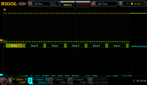
Figure 11: I2C clock data with reduced noise using bandwidth limit on a RIGOL MSO5354 Digital Oscilloscope

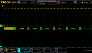
Figure 12: I2C clock and data using high resolution mode on a RIGOL MSO5354 Digital Oscilloscope


Signal Quality
Monitoring and improving the quality of low speed serial signals is a critical part of the debugging process. Issues like impedance mismatches, bandwidth, and loading errors can all effect the quality of signals even when noise isn’t present. Now that we are looking more closely at the exact nature of these signals it is important to verify the way we are using our oscilloscope for these tests. For signal quality tests we will be using the analogue channels because they provide the best look at what is actually occurring with our signals. This requires some additional forethought. To clearly see data transitions, we should definitely use a sampling rate that is as high as possible. Sampling at 5x the bit rate of the digital bus should be considered the minimum because of the high frequency components that we need to visualise. Sampling at 10 times the bit rate should enable us to see

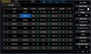
any of the issues. But when we decode the signal the scope likely uses a subset of the full memory data to handle the decode analysis. This can be important because you don’t necessarily want to decode being performed at too high of a rate. That can mask problems you will find when a more nominal receiver is used to decode the data. On RIGOL scopes the decode is done on 1 Mpts of memory spread across the acquisition. By setting the memory depth and the time per division the user can determine whether they want the decode to be done directly from the analogue points or from a subset. Decoding is also shown across the display region. To capture more decoded bytes than you can view on the display use the event table function (Figure 13). You can also export the table results to a text file from the event table menu for record keeping or offline timing analysis.
Here is an example table of how the memory depth, time per division, and sample rate effect the actual decode sample rate on a MSO5000 Series. Based on your serial data speeds and the receiver you will eventually use to collect the serial data you can optimise your serial decode rate.

Now that we have set and verified our sampling times for best analogue and decoding results, we also want to set our display up for optimal triggering conditions. When triggering on the rising edge of an analogue signal make sure to keep the trigger level at least 1 division away from the signal low state. This separation allows for consistent

triggering action without any false triggers. When visualising digital signals with the analogue channels use more screen real estate when possible. Using about 2 vertical divisions and about ½ to 1 horizontal division per decode character will allow you to see any major overshoot or impedance issues as well as some of the other types of error we will be looking at. Here is the setup (Figure 14) I prefer to monitor decoded data on a bus like RS232.
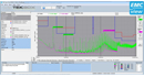
On a more complex bus like I2C we view both clock and data lines on the screen. The timing correlation between multiline buses is, of course, vital to successful decoding. Making critical measurements on the screen like risetime and overshoot for each line makes reliability tests simple to setup. We can view the measurements in max/min or using standard deviation notation for more advanced statistical testing (Figure 15).
In addition to the risetime and overshoot for the 4 serial bus lines you can also see the jitter in the clock when compared to the data transition. This test device appears to have the clock transition occur about 1.6 microseconds of jitter on the clock when viewed, as above, in reference to the triggering data transition. In (Figure 16) we zoom in on the data transition to get a more accurate measurement of the risetime and overshoot.
Signal quality encompasses many of the types of issues you find on LSS buses. Efficient debug means making the most of your embedded analysis capabilities to find signal discrepancies that can lead you to design changes as early as possible in your design process. A mixed signal oscilloscope is the perfect tool for measuring signal quality (Figure 17) from risetime variance to ASCII packet data.

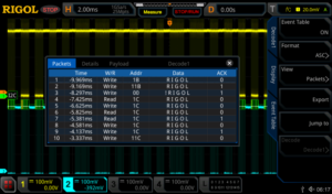
Figure 13: I2C clock and data event table view using a RIGOL MSO5354 Digital Oscilloscope

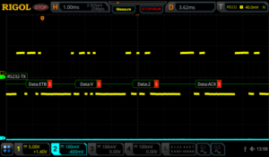
Figure 14: RS232 optional decoded data view settings using a RIGOL MSO5354 Digital Oscilloscope

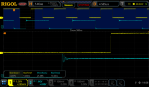
Figure 15: I2C clock and data min/max signal measurements using a RIGOL MSO5354 Digital Oscilloscope

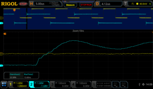
Figure 16: I2C zoom in on data risetime measurement using a RIGOL MSO5354 Digital Oscilloscope


Data
The key to any Low Speed Serial application is the ability to quickly and easily look at the data being transmitted. This means adding the capability to do embedded decoding on your oscilloscope. Decoding affects both the triggering and display on the scope. It adds a decoded bus display to the instrument’s screen. You can decode values as ASCII or as hex, octal, or binary data depending on what you want to look at. You can also trigger on these values to make sure you are looking at the packets of most interest to you (Figure 18). In addition to triggering on these signals with the decode specific trigger you are also able to trigger on any type of signal with a zone trigger which allows you to not only to trigger on any type of signal but also exclude any unwanted noise or data from a signal. These are created by simply drawing a rectangle on the screen of the instrument (Figure 19).

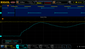
Figure 17: I2C data measurements with standard deviation using a RIGOL MSO5354 Digital Oscilloscope

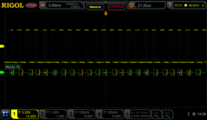
Figure 18: RS232 optimal decoded data view settings using a RIGOL MSO5354 Digital Oscilloscope

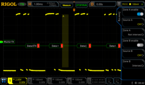
Figure 19: A zone trigger is added to exclude part of the RS232 signal.

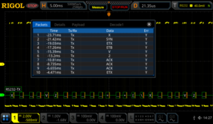
Figure 20: RS232 event table capture of multiple transmissions using a RIGOL MSO5354 Digital Oscilloscope


If you are interested in timing between packets or evaluating more than one or two consecutive packets of data, use the event table mode (Figure 20) to generate a list of data packets on a wider time base. Additionally, with using an event table you are easily able to move around on the decoded signal by stopping the instrument from sampling and then select your desired trigger point in the packet’s submenu on the event table then press the Jump To button to move to the desired trigger point on the captured signal (Figure 21).
You can always utilise the zoom function to see the signals and data from an individual packet in that series (Figure 22).
Another way to view this signal is by using the search and navigation menu. This allows you to view multiple trigger points and easily move around on the signal when the scope has stopped scanning. All of the trigger points are represented on the search and navigation menu and they correspond to the white triangles at the top of the screen. The trigger point that is highlighted on the table corresponds with the red triangle at the top of the screen (Figure23).
To view how decoded segments, differ over time or compare between triggered events when other signals might be affecting the results the best analysis method is often to use record mode. RIGOL’s record mode enables you to capture thousands of frames around a trigger event. Once captured, you can use pass/fail or a trace difference analysis mode to visualise changes from frame to frame (Figure 24).

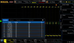
Figure 21: RS232 Event used to move around on the signal by using the Jump To soft key.

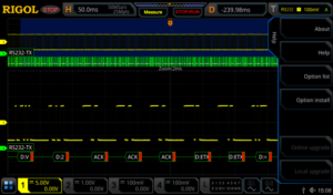
Figure 22: RS232 packet view using zoom mode on a RIGOL MSO5354 Digital Oscilloscope

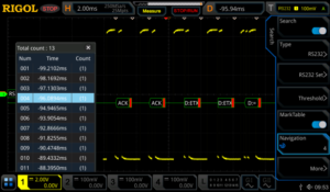
Figure 23: Using Search and Navigation feature to move around on the RS232 signal.

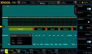
Figure 24: I2C with pass/fail analysis enabled using a RIGOL MSO5354 Digital Oscilloscope


These recordings can be stored and played back as a movie as well, but the analysis features let you search for failures or outliers while also viewing decoded data for comparison (Figure 25).
Data errors as well as the debugging process are always closely tied to the protocol and its specifications. To be efficient with your test equipment make sure you are utilising the best analysis method to easily view the data you need to see without extraneous results getting in your way.

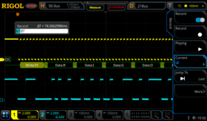
Figure 25: I2C transmission record mode in playback using a RIGOL MSO5354 Digital Oscilloscope


Keys to Look Out For
Proper Oversampling & Bandwidth
As discussed, proper sampling is critical to making correct measurements as well as completely debugging your low speed serial signal. A good rule of thumb for analogue signals is 5x the bandwidth of the signal you want to measure. This limits your risetime error to about 2%. To view the best detail on high frequency signal components set up your scope to achieve 5-10X over sampling as well. When digital signals this means sampling 5 times in the width of one bit. When sampling on digital lines or for sampling that will be used for decoding oversampling is less important but set up your measurement device so it is as similar as the LSS receiver you will ultimately be using. This gives you the best chance to focus on material errors that will cause problems down the road.

Grounding, Noise, and Differential Signalling Proper probing and understanding the use of
differential vs. ground referenced signals is important to debugging. If your data lines are not ground referenced make sure to understand the impact of ground loops and ground coupled noise on your measurements. Use proper probe techniques and advanced noise cancelling features on the scope to limit noise sources. If necessary, add differential probes to your measurement system to improve measurement quality.
How to Best View Low Speed Serial Signals There are a number of methods for analysing,
viewing, and evaluating LSS bus activity on a modern oscilloscope. The best way differs depending on whether you want to look at a single bit transition for noise, speed, or synchronization; whether you want to look at a complete packet of data; or if you want to compare packets and packet timing over a longer time period. Make sure your bench tools allow you to see everything you need and familiarise yourself with features like zoom, record mode, search and navigation, event tables, deep memory, and automatic measurements as well as how they interact and how best to transition between them when considering your test plan. Ideally, an oscilloscope empowers you to view all the results you need and quickly switch modes to acquire additional information.

Conclusions
Embedded design and debugging of digital data is a growing test requirement in a broad range of consumer and industrial applications. Having the right mixed signal oscilloscope can make viewing, analysing, and resolving issues including timing, noise, signal quality, and data easier and faster. This improves engineering efficiency and time to market. RIGOL’s line of UltraVision II enabled oscilloscopes comes with standard or optional capabilities for the methods and measurements discussed here and are powerful benchtop instruments that provide uncompromising performance at unprecedented value.

Products Mentioned In This Article:

  • DSA815 please see HERE
  • MSO5000 Series please see HERE
  • RP7150 please see HERE

Kikusui PCR-WE/WE2 Series Application Software

Posted on: May 18th, 2021 by Doug Lovell

For the full PDF of Application Software for the PCR-WE/WE2 Series AC/DC Power Supply please click on the PDF image below.


Kikusui PWX Series – Take control of your Power Testing.

Posted on: May 17th, 2021 by Doug Lovell

Kikusui PWX DC Power Programmable Supply – 750W or 1.5kW, LAN , RS232, USB and rack-able

PWX is a new series of DC power supply in only 1U height, for rack or bench use. With outstanding power per volume, all models allow Constant Volts or Constant Current operation. A 19-inch wide geometry allows close stacking on top of each other is achieved by cooling design with air flowing from the front to the back. With USB, RS-232C, and LAN interfaces as standard, an essential for system upgrades, PWX PSUs come complete with virtual multi-channel bus (VMCB). This facility supports many architectures for remote control and monitoring: 1-to-N, or N-to-M topologies, thereby supporting very large-scale applications. With a network interface offering LXI compliance*, it is easy to monitor and also to control your power supplies from any networkable browser: a PC, smartphone, or tablet, for example, bringing freedom of location to your systems management.

Powerful yet simple configuration via PWX’s LAN interface
To configure PWX, simply connect your PC, or route to the PWX via a hub, using a LAN connection. If you want to work with many machines in specific combinations, create a virtual group using the VMCB features: up to 255 virtual groups are configurable, and up to 31 units per group. A group can have a mixture of models you need.

Easy monitoring and control of a live PWX using built-in web server
As well as setting up, the browser on your PC and many smartphones/tablets can also be used for active control and live monitoring. Simply access the applications for control on the web server built into the PWX series.

Wide Operating Range: up to 3-times the capability – see chart operating region
A wide range of voltage and current outputs are available from PWX, via output power auto-ranging (a factor of three across the range). For example, the 1500 W output power model PWX1500ML functions continuously across the range of ‘80 V-18.75 A’ to ‘26.8 V-56 A’.

Sequence Creation Application Software SD013-PWX (Wavy for PWX)
Automated testing applications are accommodated using the optional Wavy for PWX. The Wavy application software enables sequenced data to be edited and uploaded to the PWX for complex testing solutions.

Kikusui’s new PWX Range includes this wide range of DC power instruments:

PWX750LF – Wide Range DC Power Supply 1U 750W, 0~30V/0~75A
PWX1500L – Wide Range DC Power Supply 1U 1500W, 0~30V/0~150A
PWX750MLF – Wide Range DC Power Supply 1U 750W, 0~80V/0~28A
PWX1500ML – Wide Range DC Power Supply 1U 1500W, 0~80V/0~56A
PWX750MHF – Wide Range DC Power Supply 1U 750W, 0~230V/0~10A
PWX1500MH – Wide Range DC Power Supply 1U 1500W, 0~230V/0~20A
PWX750HF – Wide Range DC Power Supply 1U 750W, 0~650V/0~3.5A
PWX1500H – Wide Range DC Power Supply 1U 1500W, 0~650V/0~7A

Full specification in pdf: Click HERE
Telonic Instruments Ltd. is a stock holding distributor able to provide many models quickly.
A hire option is also available for many instruments from Telonic Instruments Ltd.
For more information:
Telonic Instruments Ltd Telonic is an ISO9001 Registered company.

Phone
0118 9786911
Fax
0118 9792338

Web Address
www.telonic.co.uk

Siglent’s NEW SSG5000X Series 4GHz / 6GHz RF Signal Generators!

Posted on: May 15th, 2021 by Thomas

Siglent’s SSG5000X Series of Signal Generators can generate analogue and vector signals, and have a frequency range of 9kHz to 4GHz/6GHz. They feature the industry-leading performance in phase noise, spectral purity, bandwidth, EVM and output power. The internal IQ modulation generator and waveform playback function make it easy to create even the most complex signal types. They also cover the most important RF band for digital wireless communications and include standard waveform files. The Siglent SSG5000X are powerful and cost effective sources that are ideal for R&D, Education and Manufacturing.

SSG5000X Series >>

RIGOL´s new Solution for EMI pre-compliance tests

Posted on: April 26th, 2021 by Doug Lovell

VNA Mode for Real-Time Spectrum Analysers

Enhanced EMI measurement function and a simple user-friendly operating environment complete RIGOL’s real time spectrum analyser versions RSA3000N and RSA5000N.

Electromagnetic compatibility [EMC] has become one of the most important topics in the last 23 years. EMC activities during design phase are absolutely mandatory to ensure the functionality of development and to protect the environment from electro smog. Each new development must be tested in a test laboratory in accordance with related standards in order to be CE certified. This certification is necessary to bring a new product to the market. Different standards are used depending what kind of product is designed. For example standard CISPR 22 (EN55022) needs to be passed for an “information technology equipment” [ITE] like a MP3 player or a modem (telecommunication). Each standard specifies frequency ranges for conducted and radiated emission of a product and defines maximum limits in dBµV for each analysis. Pre-compliance analysis is very important during design stage because it’s estimated that ~50% of products fail the first acceptance test. A second full compliance test is very expensive and time consuming. But also a re-design has a strong financial impact and uncalculated additional time is necessary which is a question of cost in the end as well. In order to avoid this scenario, initial EMC analysis and measurements are necessary at a very early stage of development and must be carried out throughout development, including pre-compliance checks. A survey1 shows that the average cost of EMC activities during development is at ~3-5% of whole development cost. However, if these activities will not be performed and the compliance test is failed, the cost of post- development can be arise up to 50% to 100% of the actual planned cost. For EMC analysis and pre-compliance control, RIGOL has been offering since years solution with spectrum analysers of the series DSA800 (including 6 dB filters and quasi-peak value detector [QP]) and PC Software S1210, as well as a near-field probe set NFP-3. This solution has now been extended and optimised in the RSA3000N/RSA5000N series. This makes it possible to simplify EMC analysis considerably and also offers even more advanced analysis capabilities.

EMI Problematic

EMC2 was implemented to generate a peaceful coexistence between transmitter and receiver of electromagnetic energy. Also unwanted transmitting and receiving are within this definition. Furthermore EMC should protect the recourse “electromagnetic spectrum”. Three main elements are defined in EMI (see figure 1).

Source of Interference – Coupling Path – Susceptible Device

The source of interference could come from e.g. parasitic back coupling effects from an amplifier or an electromagnetic transmission of an electric / electronic facility. Due to different coupling path the disturbance will be coupled to the susceptible device. This interference could cause different failure rates in functionality at the EMI receptor (susceptible device):

1.) Performance degradation
2.) Function failure
3.) Equipment damage (worst case)

To avoid such kind of scenario it is important to detect the root cause including coupling mechanism at DUT. The EMI interferences could be transmitted via different coupling path. For lower frequency ranges the interferences are mainly transmitted via line connection (like for power, data bus, analogue lines, RF connection) because the wavelength (λ)3 is bigger than the geometry and electrical and magnetically field are independent. Both fields don’t propagate and a quasi-static approach is necessary (analysis of inductive / capacitive elements). The line connections need to be tested if unwanted interferences occurring during / after activation of DUT at these lines. This kind of test is named conducted emission.

When the wavelength of a DUT is equal or smaller than its frame, then magnetic and electric field are no longer independent and they start to combine to an electromagnetic field (EM). If e.g. the geometry has 6 * λ then the EM field is no longer only at the source, propagation happens and the DUT start to send out an EM wave (its acting as an antenna). Unwanted interferences with EM waves are named radiated emission. In the near field of the EM source a quasi-static approach is necessary.

The occurrence of interferences is in most cases unforeseen and difficult to detect because different coupling effects could be root cause of interferences. For a device under test there are two main influences of interferences. First one is an interference which is related within one DUT and has an influence of functionality within the device under design. These interferences are intra-system disturbances which will be occurred e.g. crosstalk effects.

On the other side, the DUT might be affecting a complete different independent system with EMI interferences which are inter-system disturbances. For example, at a radio it could be happened that a specific noise is hearable over the speaker when a mobile phone is ringing.

Interferences could be coupled by:
– Galvanic coupling (G-C): when two electric circuits using same impedance (e.g. same GND)
– Inductive coupling (I-C): when two (or more) conductor loops with current flow influence each other with magnetic field
– Capacitive coupling (C-C): when two electric circuits have different voltage potential – Electromagnetic coupling (EM-C): Wavelength is smaller than the geometry and EM wave radiated to environment of DUT and / or other sections of DUT.

To find a root cause coupling path in a DUT is very difficult, because coupling path could also be a combination of different couplings (e.g. G-C and C-C. at the same time). To find a solution for a detected coupling path is comparatively simple.

The next part of this document describes the test tool RSA5000N with the new EMI mode which is the tool for pre-compliance analysis.

EMI Mode of Real Time Spectrum Analyser RSA5000N / RSA3000N
The RSA5000N / RSA3000N are multifunctional spectrum analyser including a general purpose spectrum analyser [GPSA], a real time analyser [RTSA], a vector signal analyser [VSA], vector network analyser [VNA] and an EMI mode for pre-compliance tests. Therefore these devices are the best combination of high performance and flexibility and an optimal test solution for EMI pre-compliance analysis. For some EMI measurements, the real time mode could be a big benefit for some analysis to get a better overall picture of the problem or see more behaviour of DUT. The GPSA mode could be used to measure single components of a DUT like an amplifier and with VSA mode, the modulation quality or BER of an RF output could be measured e.g. during susceptibility stress.
The new EMI mode offers a lot of new functionalities and advantages for pre-compliance tests and will be described in detail:
Scan Table
During the conformity check (conducted and radiated emission / susceptibility), a test receiver [TR] is generally used in a test laboratory. However, a TR has several disadvantages. It is a very expensive test tool and only usable in the field of EMC. A spectrum analyser [SA] on the other hand, measures faster and can be used for different applications and is significantly cheaper, especially at RIGOL. However, a TR has significant advantages in EMC measurements comparing to an SA. TR using a pre-selection which allows to use a different dynamic range for each partial measurement. In addition, the desired frequency resolution (usually RBW/2 and sometimes RBW/4) is easily achieved in a TR. The SA fulfils the most of CISPR 16.1 requirements and the results are a very good approximation, which is absolutely sufficient to perform pre-compliance tests. A TR fulfills CISPR 16.1 for 100% and can also be used for compliance tests. RIGOL´s new EMI solution in the RSA5000N / RSA3000N compensates most of the disadvantages with the scan table. The most used frequency ranges inclusive the correct 6 dB RBW filter for EMC tests are pre-defined in 10 individual ranges (see figure 2). All pre-defined settings can be modified / stored according to the own need. In order to compensate these disadvantages in a SA, the EMI solution of RIGOL stores the basic setting of the most important frequency bands, including the 6 dB RBW required, in a scan table in advance (see figure 2) in individual areas [Ranges]. All parameters can be adjusted separately per area according to your own wishes.

For example, it is possible to use up to 10,000 measurement points per area. The basic settings of measurement points refer to a frequency resolution of RBW/2. For a higher resolution, different ranges can be combined for one test. With a combination of e.g. 3 ranges it is possible to use 30.000 measurement points over the whole frequency to reach expected resolution if necessary. The integrated pre-amplifier (option) and internal attenuator (0 to 50 dB) can be varied per range as well. With combination of different ranges it is possible to increase the dynamic range of the complete measurement without interrupting the measurement itself, because the dynamic range can be adjusted for each single range. The disadvantage of frequency resolution and dynamic range in an SA can be compensated in EMI mode. Additionally to the standard 3 dB RBW filter, the EMI solution contents also the integrated 6 dB filters (200 Hz, 9 kHz, 120 kHz and 1 MHz). Especially RSA5000N providing real time and vector signal analysis capabilities, which is not the case with a TR.
Integration of Limits According to Standards
After the desired frequency range has been selected, you can load the pre-defined and stored limit lines of the desired standard (e.g. EN55022, Class B, AV or/and QP) and display it on the fully logarithmic trace display. A measuring curve can be assigned to each limit. It is possible to activate a measurement curve with a separate detector setting for each pass/fail limit. Different measuring curves can also be measured at the same time. For each limit line it is possible to activate an additional security margin, which is considered in the Pass/Fail viewing. Especially in the pre-compliance check the result should be at least 5-6 dB below the defined limit line to ensure, that the compliance check will be passed.
Advanced Meter/Additional Detectors/Corrections
Another advanced measurement mode is the measurement meter. It is possible to activate up to 3 meters in parallel. Each of them can be used with different detectors and separate limit values. For example, the peak value detector [peak] can be set for first meter, second meter is set to QP detector and third meter to the new CISPR Average [C-AV] detector. The respective measuring meters can be set to the peak under focus via meter marker. The meters measures continuously. This means, for example, with an elevated peak value, the DUT can be reworked and the influence on this value can be immediately represented. A design improvement is immediately visible. With using three meters in parallel it is possible to see the peak measurement (worst case) but also the repetition pulse rate of this signal over a certain time with QP detector can be displayed. In addition a weighted average detector can be used for pulsed sinus-shaped signals with low repetition rate (C-AV4) which displays the maximum linear average value during the measurement.
The meters can be coupled with a signal which is selected in the signal table. An additional fine-tuning of the meter frequency is not necessary. So each peak in signal table can be selected and measured by marker, as well. Alternatively, the meters could be coupled to a marker. For conducted emission tests additional components are used (e.g. line stabilization network (LISN) transient limiters, external attenuator, etc.). Each of the components has a direct influence of test result over frequency range. Therefore, it is possible to activate different corrections in RSA3000N / RSA5000N EMI mode. During the test, the correction will be respected in the result. Correction values can be stored internal the instrument, as a * .csv file. These can also be generated in the PC and loaded later on into the analyser.

Measurement
Different conditions can be set for the measurement. On the one hand, variable traces can be recorded at the same time with one or more detectors. Alternatively, only the worst case situation (peak detector) can be recorded. Afterwards each peak in the signal table will be measured with QP and C-AV detector, as well. It is no longer necessary to perform a whole trace with QP and C-AV (duration can be several hours) because these detectors are only interesting when peaks are visible and the test engineer has the information in some minutes and saves a lot of time during pre-compliance evaluation.

The number of readings in the signal table can be pre-defined. In order to get a detailed view of a peak value, a zoom is available to enlarge a detailed view of a peak. After analysis, the view can be zoomed out to get back the original view.
In case that the full screen of the trace is required, the measurement meter and the signal table can be turned off on the screen.

Documentation
In the EMI mode of RSA5000N / RSA3000N series, the measurements can be stored in different ways. For example, the complete signal trace can be stored as a * .csv file or a test report including settings, limits , an image of the graph including meter result and the signal table can be created as HTML or *.pdf in the analyser itself or on an external USB stick. It is possible to modify the header of the test report with information like temperature / humidity, name of operator or test location, etc.
The next part of this document will go through some measurement examples with conducted / radiated emissions and near field probing.
Conducted Emission
As already mentioned, conducted emission is mainly measured up to 30 MHz at lines (e.g. power, analogue / digital signals, etc.). For conducted emission test on power line it is necessary to supply the DUT with power. At the same time the disturbances from DUT shall be measured. The problematic is, that also from the power supply disturbances could be send out which shall not be measured. Another aspect is the impedance matching to avoid a wrong result based on an impedance mismatch. The solution for this problematic is the usage of a line impedance stabilization network [LISN]. A LISN blocks all interferences (via inductive component) from power supply to SA, but supplies a DUT with power. Depending on inductive size, a LISN can be used for DC (5 µH) or AC (50 µH) power source. The power will be blocked on the way to SA (via a capacitance) but the DUT disturbances won’t be blocked and transferred to the SA. The impedance at SA connection is 50 Ω.


Two security mechanisms are important using a LISN. When a LISN or a DUT will be activated, then the electric charge of capacitance changing and current flows for a short period. This transient current can destroy the first mixer diode in a spectrum analyser. It is recommended to use a transient limiter between LISN and SA, to protect the analyzer5. For the first test it is also recommended to use an external attenuator for the test to see if high disturbances will be occur from DUT. The attenuator can be removed after first test, when the user be sure, that the disturbance peaks are at a normal level.
In each standard it is defined how the test setup has to be performed. In figure 6 there is the physical connection of a test setup displayed:

The ground connection of LISN (and DUT if possible) needs to be connected to the horizontal ground plane.
In the example below the conducted emission test was performed on a power supply (Phase) of a test device using a 50µH AC LISN6. First test was performed with integrated LISN limiter and the second test in figure 7 was performed without limiter. The limit lines and detectors are selected for standard EN55022, Class B. The test result is including correction values of LISN. This test uses two limit lines. First one is for average detector and second (blue) limit line is for QP detector. For information only, the peak detector was also activated for final measurement, because the peak detector displays always the worst case value. This power supply is very close below the limit margin, but it passed. Higher peaks can be analysed via measure meter.

Additionally to EMI analysis the frequency band can be analysed in real time [RT] as well. This mode uses a very fast FFT algorithm to calculate the frequency spectrum. The calculation time is smaller than one FFT frame. Therefore a seamless capture of time signal is possible and no signal information7 will be lost. In RT mode different displays can be used. For example within density mode it is possible, to see a signal repetition over test time in different colour grades and therefore it’s possible to see more details. Density or Normal view could be combined with spectrogram (time waterfall over frequency range) where different amplitude values are displayed in diverse colour grades (see figure 8).

An additional strong tool is the combination of frequency view and power vs time (with bandwidth up to 40 MHz8) in parallel. For a SA it is only possible to view the frequency spectrum or zero span with the max bandwidth of used RBW but not both in parallel. In figure 9 the same DUT was tested with smaller frequency range and with normal spectrum in combination of spectrogram. For this measurement it’s possible to speed up test time to 100 µsec. The interference pulses are now visible in spectrogram. With a Z marker it is possible to measure the difference in frequency, amplitude and time of an interference signal.

Near Field Probing
Near field analysis is a very important part in pre-compliance analysis and root cause debugging. RIGOL offers with the set of near fields (NFP-3) 4 different H probes for failure detection (see figure 10). It is a special form of emission analysis, because the measurement is done in reactive nearfield range (up to 0.159 * λ)9. In near field magnetic and / or electric field needs to be measured separately because both have a phase shift of up to 90° and nearfield stores blind energy without radiation. For most radiated emission root causes can be detected with locating the near field strength.

Tests on housing leakage could be detected as well as strong disturbance components like ribbon cables or LCD panels. Bigger probes are usable to find the area of interferences. Smaller probes can be used to detect the exact source.
One approach for near field analysis is to use the spectrum analyser with linear frequency scale / no limit lines and test e.g. a frequency range of 30 MHz to 500 MHz with a RBW of 100 kHz and activation of pre-amplifier (internal attenuator: 0 dB) to get a first view the interference peaks of DUT (see figure 11).

Radiated Emission
According to the description at the beginning, propagation starts when λ is small to the geometry and E & H are no longer independent. Both are in-phase and propagate to the environment. Radiated emission is not easy to test. In a test laboratory a big hermetic test chamber is used where far field conditions are fulfilled and other influences (due to external components like a mobile phone, etc.) are not visible in the result. Far field condition starts with a distance of 4 * λ and the characteristic wave impedance is 120 * π Ω (= 377 Ω). The hermetic room has in most cases at the wall broadband absorber for impedance matching of EM wave to avoid reflections. The altitude of broad band antenna can be changed during a test to find the highest peak at DUT during the test10.

In most cases such kind of test chamber is not available for pre-compliance analysis. Therefore alternative ways has to be evaluated.
First of all, it is possible perform a free field measurement with the distance of radiated near field which is defined for 0.159 * λ to 4 * λ. In this region a far field evaluation is possible (with using correction values). To detect the test area attenuation11 from environment it is possible to perform a test with a counter antenna instead of DUT and the results will be compared with defined formula of theoretical value. The difference is the test area attenuation. Depending on the distance between antennas, variable correction factors are used. This test needs a very good conductive ellipsis area12. There shall be no conductive obstacles greater than 5 cm within the ellipsis (see figure 12). DUT and test antenna are located within the focus of ellipsis. It is necessary to perform an altitude variation of test antenna to detect maximum.

This test is very time intensive and expensive. A more simple way of radiated emission analysis for pre-compliance test is, to use a TEM cell.

A characteristic for radiation of antennas is the far field. According to the description above, the characteristic wave impedance ZF = E / H which is in far field, is 377 Ω. The idea of a TEM13 cell is the medium of a coax cable which is suitable for a TEM wave propagation. The characteristic wave impedance in a coax cable is independent of the mechanical structure and always 377 Ω. A TEM cell is displayed in figure 1314. A common use for pre-compliance analysis is, to use an open TEM cell with disadvantage to see influence from environment. But this could be evaluated as a reference measurement with deactivated DUT. The two bends on the roof are necessary for the matching, but results into a frequency limit (max frequency range) is the cut off frequency based on the generation of higher wave guide modes on these bends which have an influence on test results. This cell can be used for susceptibility stress of a DUT but can also be used for repeatable pre-compliance radiated emission approximations which are sufficient for pre-compliance analysis. The connection to a spectrum analyser needs a DC blocker because the lowest cut off frequency of a coaxial cable is 0 Hz (= DC) which could destroy a spectrum analyser. For impedance matching of septum15 it is necessary to use a 50 Ω Termination on second port to avoid reflections. The DUT is placed between septum and lower shielding plate. A test setup is visible in figure 14. The advantage of open TEM cells, failures can also be analysed in parallel with a near field probe to detect the root cause area of DUT.

Susceptibility Analysis
Near field probes, current probes and TEM cells can also be used for conducted / radiated susceptibility stress of a DUT. RIGOL’s RF generator series DSG800 or DSG3000B are an optimal tool in combination with those components, to stress a DUT with an amplitude modulation [AM] e.g. according to IEC 61000-4-316, A functionality during stress might be controlled via the oscilloscope MSO8000 to see e.g. influence to jitter of clock signals or wrong decoding of bus systems or to see crosstalk effects on strip lines. Conducted susceptibility could be done with a current probe over the related stress cable. Also the real time spectrum analyser can be used to measure, in parallel, sporadic interference reaction at DUT due to susceptibility stress. The real time functionality offers different trigger types. One is the frequency mask trigger [FMT] which is a defined field (different colour) and the RTSA measures only, when the conditions of the field is fulfilled (e.g. measure, when a signal is inside the FMT field, see figure 15).

The quality of digital modulation of RF interface during absorption stress can be tested via RSA5000N VSA (see figure 16). Here it is possible to display also I and Q stream separately to see which part of transmitter is affected by the interference. Additionally a BER test could be performed during stress situation.

Additionally, with the vector network analyser function [VNA] it is possible to measure out related antennas or other components to see if a possible degradation of performance is visible (see figure 17).

Summary
RIGOL offers a new dimension of pre-compliance testing with the new EMC solution for the series RSA3000N/RSA5000N. With the additional meter measurement method high peak values can be determined and improved at a very early design stage. This test solution eliminates the need for PC test software. The EMV analysis is also greatly simplified by the pleasant operation of the device (touchscreen or operator panel as well as USB mouse or USB keyboard). In addition, the real-time capacities (real-time is integrated as standard) of the RSA series provide an expanded insight into EMC analysis.

Rigol Introduce NEW DS8000-R Series Compact Digital Oscilloscope !

Posted on: February 17th, 2021 by Thomas

Rigol Technologies introduced the new DS8000-R Series Compact Digital Oscilloscope.

The DS8000-R series is a medium and high-end digital oscilloscope with a compact size designed on the basis of the ASIC chip (RIGOL self-owns its intellectual property right) and UltraVision II technical platform developed by RIGOL. It is compact and thin in design. It supports system integration of multiple devices, rack mount installation, and remote system operation to meet the system requirements for industrial automation test system.

DS8000-R Series >>

Rigol DM3000 Price Reductions

Posted on: February 8th, 2021 by Doug Lovell

For a limited time Rigol have reduced the price of the DM3000 Series.

DM3058 was £515.00, now £453.00

DM3058E was £361.00, now £335.00

DM3068 was £633.00, now £544.00

Offer now ended

Click HERE to view the DM3000 Series Category Page

Power grid test capabilities in the field of new energy

Posted on: December 17th, 2020 by Doug Lovell

These products can be used as central devices in the power grid tests for distributed power generation with sunlight, wind, fuel cells, and gas engines.
They provide a platform for testing systems in connection with loads, electric power analyzers, and other devices.

Ideal for EMC and power supply standard tests

Posted on: December 17th, 2020 by Doug Lovell

The response speed of the PCR-LE Series internal amplifier may be selected according to the required load conditions and purpose.
Their stability for EMC test sites result in precise inspections. They are also applicable to power supply standard tests for aircraft-mounted systems that require a high level of precision.

Dependable stability and high quality output

Posted on: December 17th, 2020 by Doug Lovell

In addition to their rapid response characteristics, PCR-LE devices supply output voltage and frequency that can be changed at any time.
Because they do not generate noise like those from the PWM inverter system, they produce power supply abnormality simulations easily and with a high level of precision for research and development and for instantaneous power failure tests on production and inspection lines.

Reliability backed by a global track record

Posted on: December 17th, 2020 by Doug Lovell

The entire PLZ Series is highly regarded by a wide range of users who deal with leading-edge technologies on a practical basis in many different disciplines.
These loads have also been adopted for inspection systems by global manufacturers and research institutions involved with space development and information technology.

High precision simulated load tests

Posted on: December 17th, 2020 by Doug Lovell

These products accurately reproduce the desired discharge waveforms without using any real load.
Simulated load tests may be conducted with great precision, considerably increasing the efficiency of power supply circuit evaluation.