Introduction
Stability is one of the most important characteristics in power supply design. Traditionally, stability measurements require expensive frequency response analysers (FRA) which are not always available in a laboratory. SIGLENT has released Bode Plot Ⅱ features to the SIGLENT SDS1104X-E, SDS1204X-E, SDS2000X-E, SDS2000X Plus, and SDS5000X series of oscilloscopes. When combined with a Siglent arbitrary waveform generator (SDG or SAG) and an injection transformer, quick frequency response curves can be created.
In this application note, we will show you the basic principles for making this stability measurement and how to use these instruments to make the measurement.
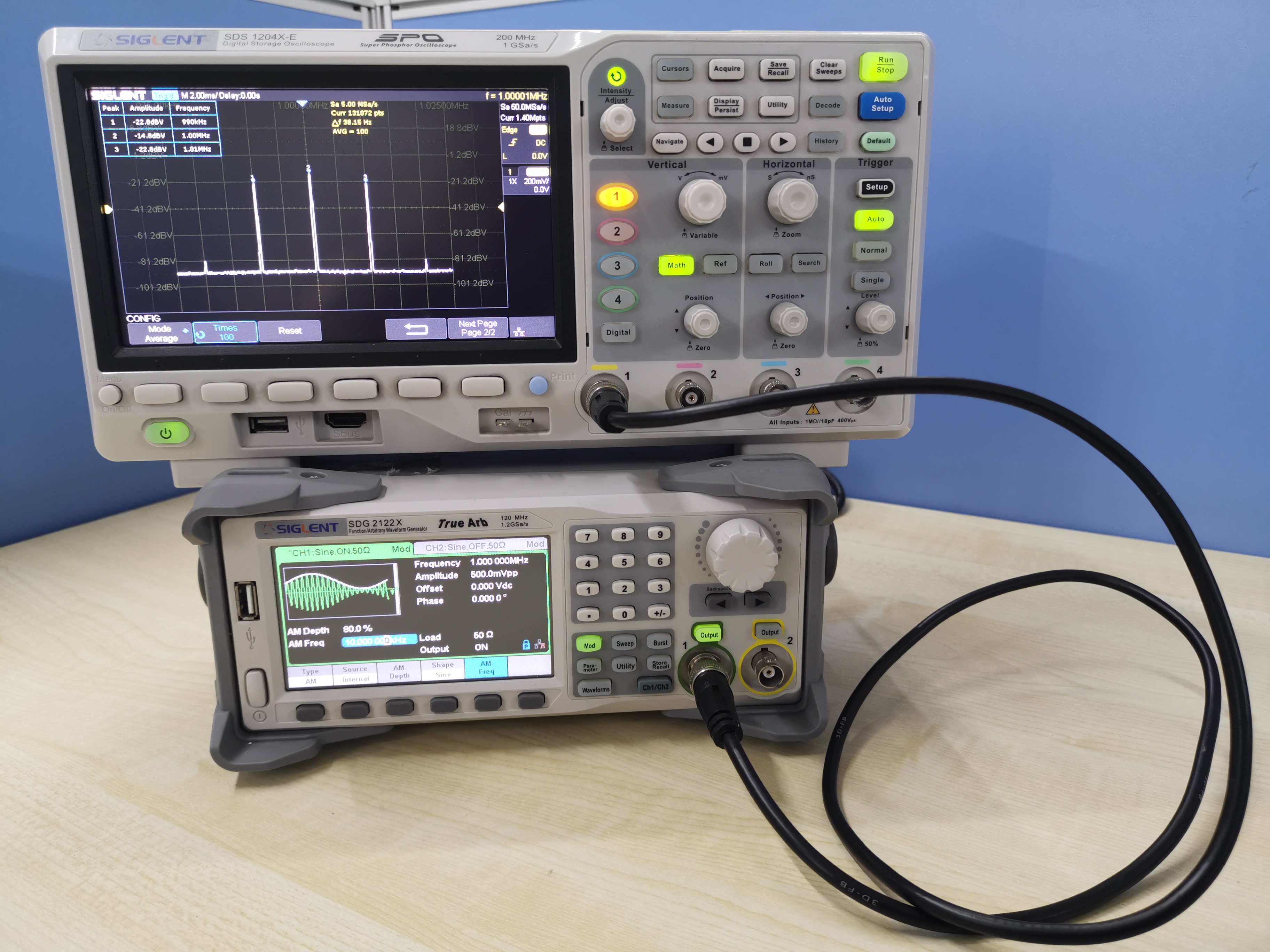
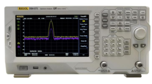
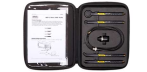
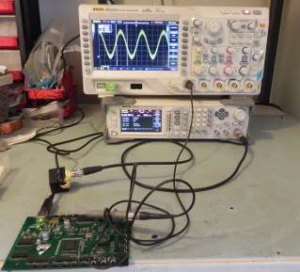
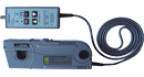
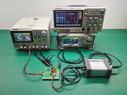 Figure 1: Bode II setup
1. Basic Principle of Stability Measurement
1.1 Stability of The Feedback System
A regulated power supply is actually a feedback amplifier with a large amount of current sourcing capability. Any theory that applies to a basic feedback amplifier also applies to a regulated power supply.
In feedback theory, the stability of a feedback system can be determined by evaluating the loop transfer function. A more practical way is to measure the bode plot of the loop gain. Figure 2 shows a typical feedback system.
The closed-loop transfer A is the mathematical relationship between input x and output y. The loop gain T, by its name, is defined as the gain of a signal traveling around the loop.
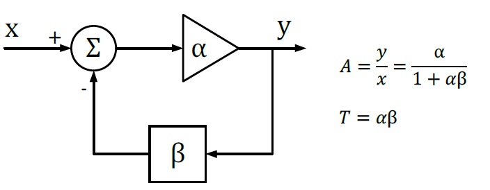 Figure 2: Typical Feedback Loop
Since α and β are complex variables, they have not only magnitude but also phase angle, as also does the loop gain T. If the phase angle of T reaches -180° while the magnitude is 1, the closed-loop transfer function A becomes infinity. In this situation, the system will maintain an output signal while there is no input. Thus, the system acts as an oscillator rather than as an amplifier, which means that the system is not stable.
If we plot the loop gain in a bode plot, we can evaluate the stability by finding the phase margin and gain margin. A phase margin is defined as how many degrees the phase can be decreased before reaching -180°while the magnitude is 1 (or 0 dB). The gain margin is defined as how many dB in magnitude can be added before reaching 1 (or 0 dB) while the phase is -180°.
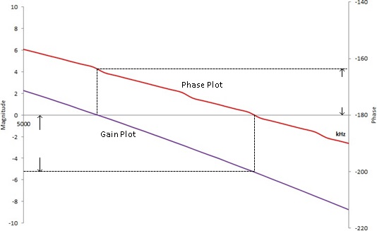 Figure 3: Bode Plot, phase, and gain margin
1.2 Break the Loop
To get the desired loop gain, we simply break the loop. Figure 4 shows how to break the loop in a typical feedback system. Technically you can break the loop any place you like. We commonly choose to break the loop at the point between the amplifier output and the feedback network. Then we insert a test signal i to travel around the loop. The loop gain is the mathematical relationship between the output y and the test signal i.
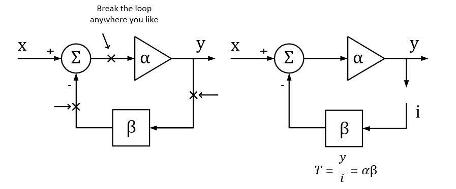 Figure 4: Breaking the loop in a typical feedback system
1.3 Loop Injection
In reality, we can never really break the loop because the feedback loop serves to maintain the DC quiescent operation point of the circuits. Without the feedback loop, the device under test will become saturated because of the small input offset voltage, and then no useful result can be measured.
To overcome this, we should measure the open-loop response inside a closed loop. Therefore, we just inject a signal into the loop rather than breaking the loop. Figure 5 shows a typical method of loop injection. The injection point is chosen so that the impedance looking in the direction of the loop is much higher than that looking backward. One possible point is between the output and the resistor divider feedback network. Other points that meet this requirement may be chosen.
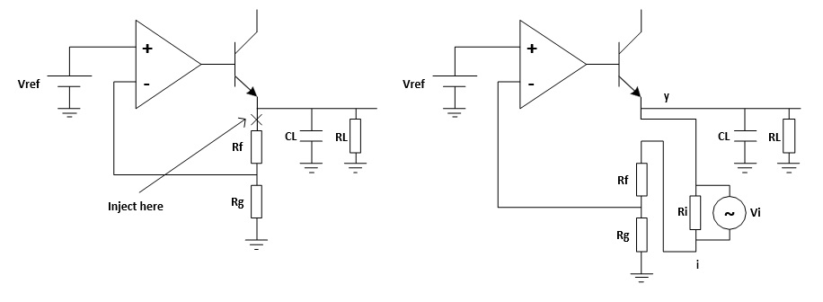 Figure 5: Loop injection
To maintain the closed loop, a small injection resistor Ri is inserted at the injection point. The resistor should be small enough so that it will have little effect on the circuit and also the lower the resistor value the lower the frequency the transformer will operate. Picotest recommends a resistor value of 4.99 Ω for the J2100A, and a larger value may be chosen depending on the circuits. The injection signal is then applied across the injection resistor.
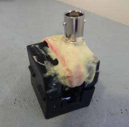
The signal injected should have no effect on the DC operating point of the circuit. A method to solve the common ground connection problem is to use an injection transformer as shown in Figure 6.
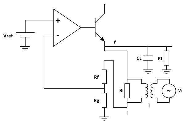 Figure 6: Injection Transformer
The injection signal starts at one end of the injection resistor, travels through the resistor divider feedback network, the error amplifier and the pass element transistor, and finally to the output, which is the other end of the injection resistor. The relationship between the injection signal i and the output signal y is the loop gain that we wish to measure.
Be aware that we are measuring an open-loop parameter inside a closed loop, the phase starts at 180°and decreases to 0°, rather than starting at 0°and decreasing to -180°. So the phase margin should be measured relative to 0°.
2. Measurement Setup and Result
2.1 Equipment
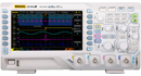
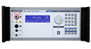
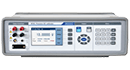
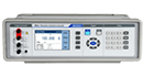
Oscilloscope: Siglent SDS1204X-E with firmware version higher than 6.1.27R1 (Bode Plot Ⅱ release)
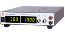
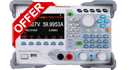
Signal Source: Siglent SDG2042X
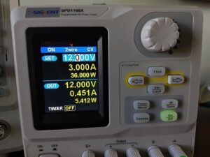
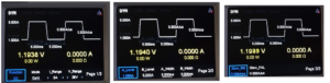
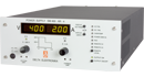
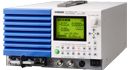
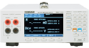
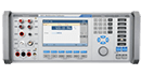
Power Supply: Siglent SPD3303X
Probe: Siglent PP215 passive probe switched to 1X
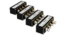
Injection Transformer: Picotest J2100A
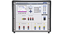
Device-Under-Test: Picotest VRTS v1.51
2.2 Circuit Connection
The Picotest VRTS v1.51 is a demonstration board for voltage regulator testing. Technically it is a linear regulator built from the famous TL431 and a discrete transistor. The schematic is shown in Figure 7. Different output capacitors can be selected to see the impact on the control loop stability.
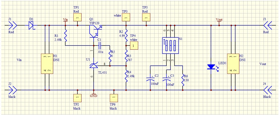 Figure 7: VRTS v1.51 schematic
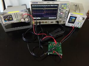
For the propose of our power supply control loop response measurement, the injection point is TP3 and TP4. The circuit connection is shown in Figure 8.
The generator is connected to the oscilloscope through USB (connection through Ethernet is also supported).
The injection transformer is connected in parallel with the injection resistor so that the signal is injected into the loop while preventing the circuit DC operation point from being affected by the generator.
The TP3 and TP4 points are also connected to the oscilloscope, and the TP4 is defined as the DUT Input while the TP3 is the DUT Output in the Bode Plot Ⅱ.
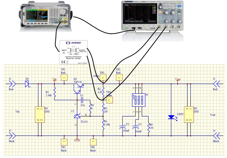 Figure 8: Circuit connection
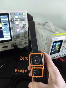
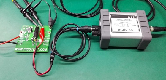 Figure 9: Probe and Transformer connections to the DUT
2.3 Instrument Configuration
In this section, we will show how the key configuration should be made in order to make the measurement correctly. For complete instructions to the Bode Plot Ⅱ, please refer to the user manual and the quick start guide.
Before entering the Bode Plot Ⅱ, it is recommended that you enable the oscilloscope’s 20 MHz bandwidth limit setting.
At this time, we want to measure the bode plot from 10 Hz all the way to 100 kHz. This frequency range should be enough for a circuit with an expected crossover frequency at about 10 kHz.
Enter the Config menu and set the Sweep Type to Simple, then enter Set Sweep to set the sweeping frequency. Set the Mode to Decade and Start to 10 Hz, Stop to 100 kHz. Set Points/dec to 20, enough for a typical sweep. Enter the Set Stimulus menu to set Amplitude to 50 mV. Enter the Set Channel menu to set DUT Input to CH1 and DUT Output to CH2.
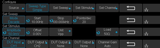 Figure 10: Bode II scope configuration
2.4 Results and Data analysis
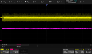
After the configuration is done, return to the main menu and press Run to start the sweep.
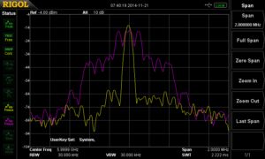
Wait to see the results as shown in Figure 11.
The result is somewhat confusing and suspect because of the trace at low frequency, especially the phase trace, alternating up and down. We will introduce a method called Vari-level to resolve this problem in the next section.
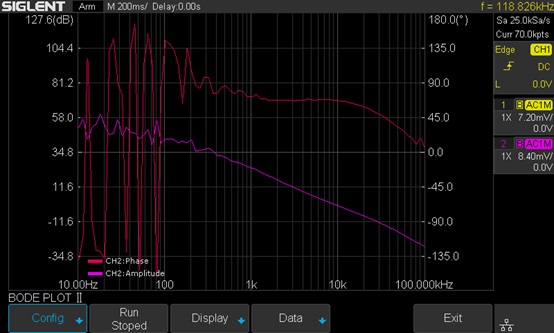 Figure 11: Measurement results
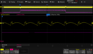
After the sweep has completed, press Run again to stop the sweep. Enter the Display menu and then enter the Cursors menu to turn on the cursors. Use the Adjust knob to move the cursors and set the phase margin as shown in Figure 12.
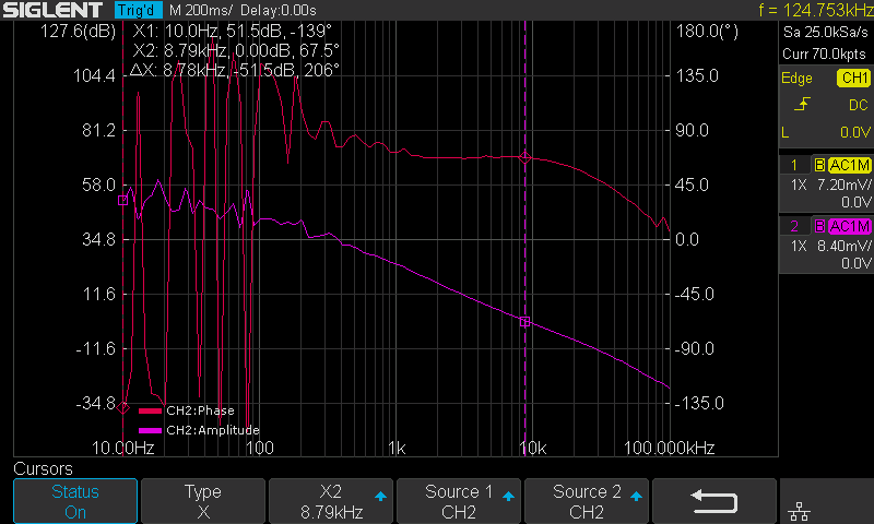 Figure 12: Cursor measurement on the Bode plot
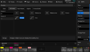
You can also turn on the List feature in the Data menu to examine the measured data, or you can export the data to an external USB FLASH driver for further analysis on a computer.
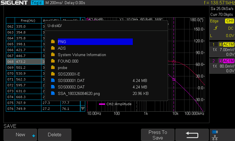 Figure 13: Exporting data
2.5 Vari-level
In the previous section, we can see that the results are not ideal, for the bouncing trace at low frequency. This is because at low frequency the amplitude difference between the input and output channel is relatively large, and since we are using a relatively small stimulus signal (this time 50 mVpp), the signal presented at the DUT Input channel is extremely small so that a commercial general propose oscilloscope cannot measure it accurately.
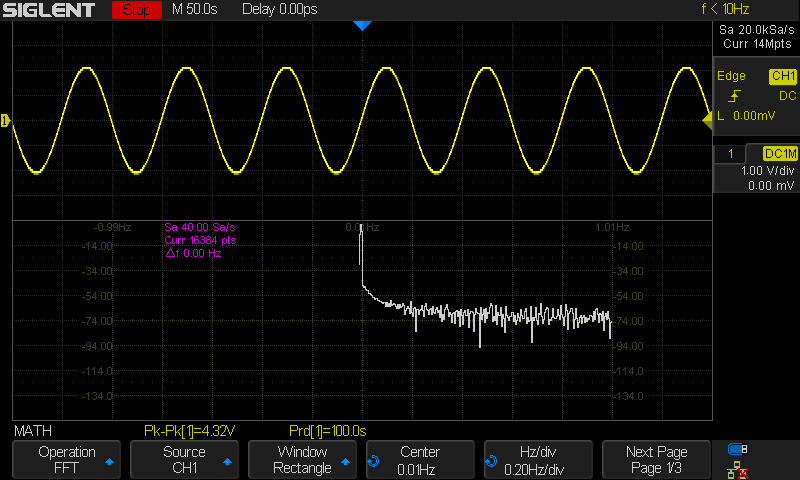
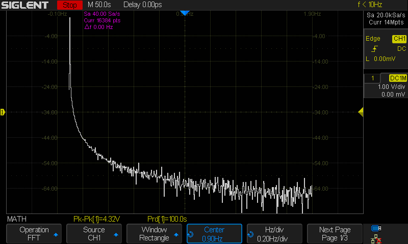
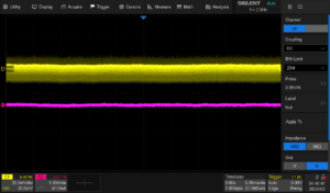
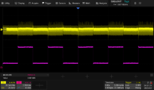
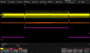
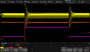
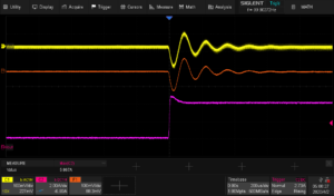
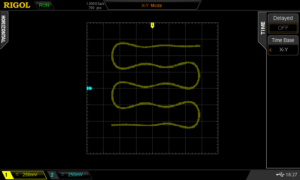
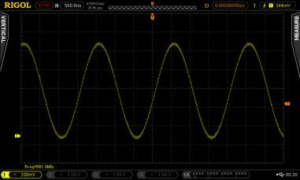
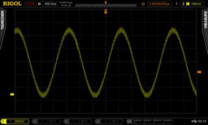
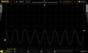
But we cannot simply increase the stimulus’s signal amplitude. The result will be similar to what is shown in Figure 14. The large signal near the crossover frequency region causes serious distortion to the loop. The distorted signal in the time domain is shown in Figure 15.
Remember that a bode plot only makes sense in a linear system, and has no meaning in a heavily non-linear system. The result is useless.
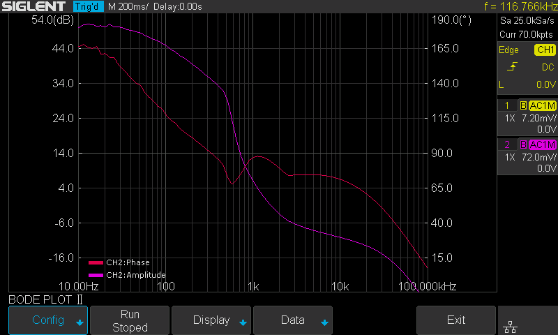 Figure 14: Increased stimulus signal amplitude and distortion
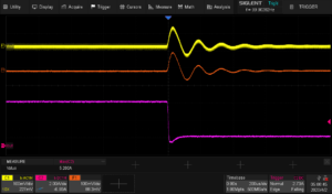
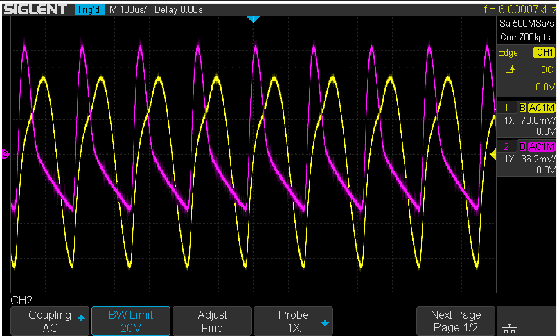 Figure 15: Distortion in the time domain
One possible solution to the problem is Vari-level (other manufactures may call it “Shaped Level” or “Level Profile”). The Vari-level concept is simple: The stimulus signal amplitude is variable over the frequency. If we use a large signal at low frequencies and decrease the amplitude to a fairly small level near the crossover region so that it causes little distortion to the loop, in theory, we can get an ideal result.
Under the Configure menu, set Sweep Type from Simple to Vari-level, and push Set Vari-level to enter the Vari-level profile editor.
 Figure 16: Set Sweep Type to Vari-level
Figure 17 shows the Vari-level profile editor. The Profile option allows the user to select and save up to 4 profiles. The Nodes sets the number of nodes in the profile trace, the minimum allowed number of nodes is 2 because at least 2 points can determine a line, and always the first and the last node set the start and stop of the trace. Press Edit Table will enter the profile editor mode. The parameter under editing is highlighted by cursors, and next push Edit Table again to cycle the cursors between “Freq”, “Ampl” and the entire row, which allows the user to navigate through the entire table. Users can use the Adjust knob to set the highlighted parameter, and pushing the knob will call out a visual keypad that allows direct input to the parameter. The Set Sweep and Set Stimulus option is somewhat similar to that in the Simple type of sweep, but they are not correlated. This time we set the sweep Mode to Decade and a 40-point-per-decade is sufficient. The profile shown in Figure 17 is used in this measurement. It is not the optimum profile for this circuit but should be a good place to start.
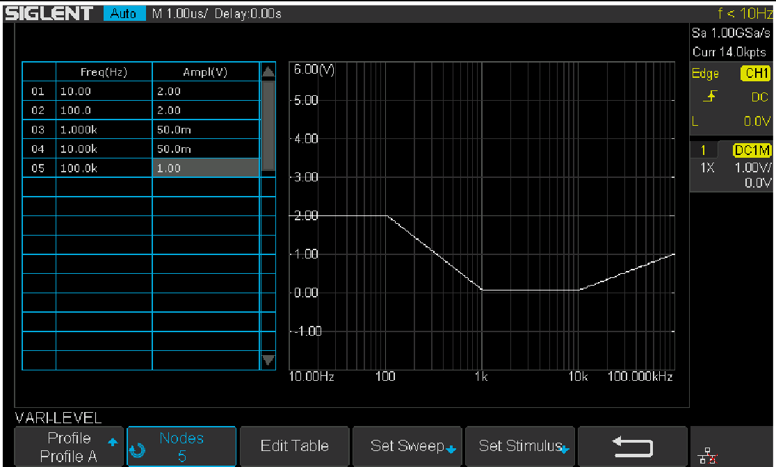 Figure 17: Vari-level profile editor
In practice, one should always experiment with those parameters to find an optimum solution for a particular circuit.
One practical way to do this is to monitor the signal in the time domain, decrease the amplitude of the stimulus signal until no visible distortion can be observed, then decrease the amplitude by another 6 dB. Next, record the amplitude and frequency, jump to another frequency and repeat the process.
There is a better way to find the optimum profile if you already have a known good profile. Reduce the signal amplitude by 6 dB and run a sweep to see if the plot changes. If it does change, reduce the amplitude by another 6 dB and sweep again. Until the result doesn’t change, then you can increase the amplitude by 6 dB and that’s an optimum profile. This is time-consuming but necessary to get a meaningful result.
Once profile editing is completed, return to the main menu and push Run to start the sweep. Figure 18 shows the final result of the measurement with Vari-level. Changing the capacitor selection switch S1 on the VRTS v1.51 demo board will alter the loop response due to the impact of different capacitors.
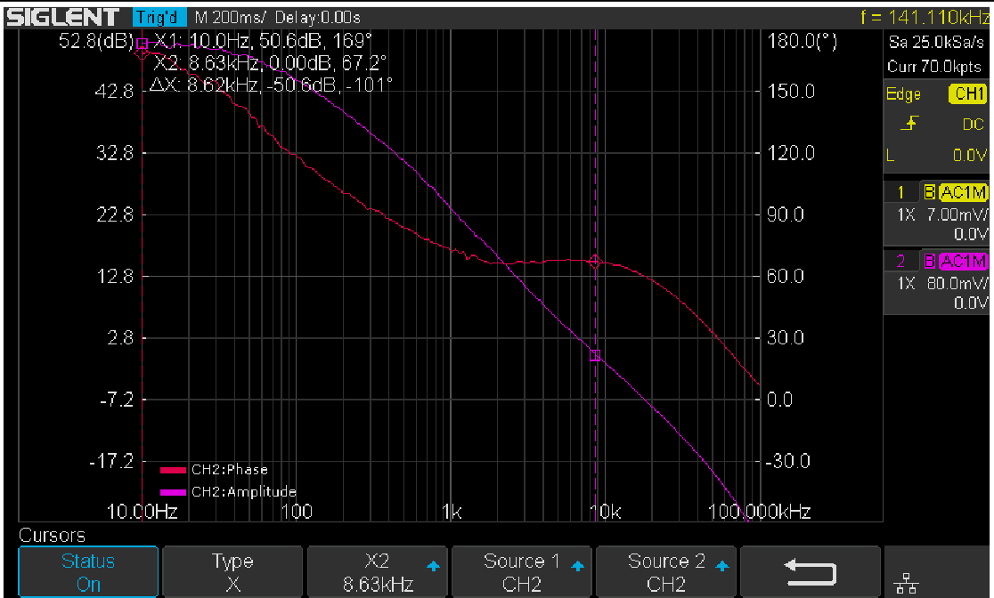 Figure 18: Results with Vari-level
3. Summary
The Siglent oscilloscope with newly released Bode Plot Ⅱ together with a Siglent signal generator and a Picotest injection transformer offer a very flexible and easy-to-use power supply control loop measurement system.
Products Mentioned In This Article:
- SDS1204X-E please see HERE
- SDG2042X please see HERE
- SPD3303X please see HERE


 FREE SHIPPING £75+
 CELEBRATING 50+ YEARS
 PRICE MATCH GUARANTEE
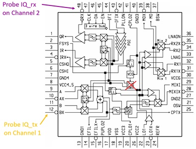
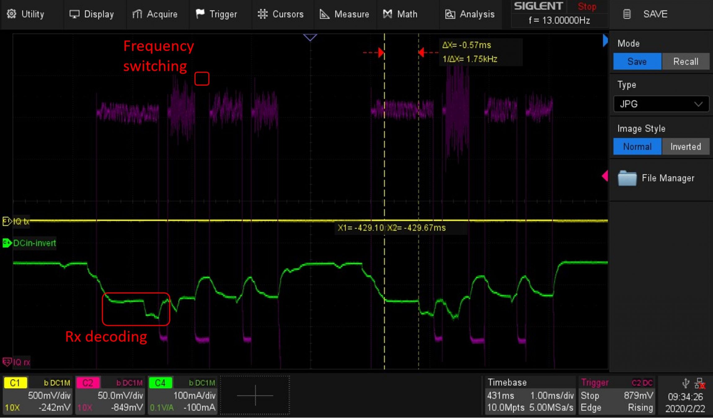
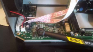
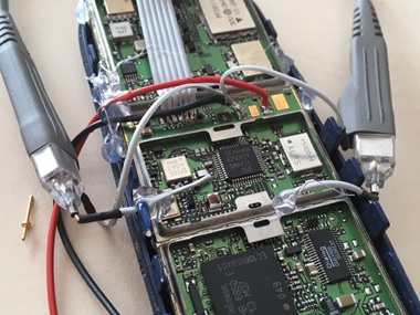 Figure 1: probing IQ signals in Tx and Rx path of the Siemens A36