


Introduction
As the Internet of Things continues to expand to include applications including home automation, fitness, video, and tracking as well as traditional embedded electronics use cases the needs for testing and optimising these designs become clearer. Even as IoT expands, the test requirements have begun to crystallise into a set of capabilities that can assist a design team in achieving their goals. This is especially important given the smaller, more versatile teams and companies charting a path in IoT. As companies and engineers often new to large scale design work attempt to make new types of successful consumer products, IoT projects will continue to progress in fits and starts until designers find the optimal mix of form and function for each target audience creating reliability and annoyances like additional time required to charge the IoT device. By first considering test requirements as a method for evaluating these concerns, a design team can speed time to market and ultimately reduce the iterations required to create a successful product platform. Selecting the best test equipment for the task at hand also enables engineers to stay within their start-up budget requirements. Signal integrity is a key design aspects whose importance is magnified by these inherent trade-offs in the IoT landscape. Focusing on signal integrity as a key indicator of the optimal approach for an IoT application from debug through final design enables a small IoT design team to leverage their capabilities and ultimately reward their customers with performance and ease. Here we will be discussing important examples of signal integrity test methodologies for IoT devices and how they impact the user experience from form to function.
From and Reliability
It is crucial to consider how dramatically signal integrity and reliability are affected by mechanical implementation. The trend for IoT products, especially wearables, continues to be sleeker, lighter, and smaller. Optimising the form of the product for users is therefore often in conflict with reliability, ruggedness, and signal integrity requirements. Designs that strike a balance too close to the aesthetic ideal often fail to succeed for these core functional reasons. With more demand for waterproof and rugged designs that also integrate accelerometers and other sensors we create an environment on our device where signal integrity can often be compromised. This can lead to shorter battery life, user feedback delay, and even critical data or system faults.
Let us test a few examples looking for issues in communication on our SPI peripheral bus. The SPI bus is a common communication protocol for accelerometers, GPS chips, and many other sensor and actuators. Continuously monitoring a design to make certain reliable communication will be maintained to quality standards is an important test technique for this type of product development. In these tests, we will provide several methods for verifying and comparing SPI communication that can be used iteratively as your design approaches completion.
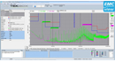
First, there are several aspects of serial communication that can be commonly affected by connections, layout, and stress or other aspects of long term use. These include bandwidth, noise, and impedance. Again, our first goal is to establish both a goal and a baseline for these parameters. The first step is to monitor and verify these signals with the analogue channels of an oscilloscope as shown in Figure 1.
In this test we can see that our connections appear to have more than enough bandwidth but we can also see some crosstalk noise especially on the data and chip select lines. The green bus values are an internal decode of that signal by the scope. As long as these are stable for each transmission then the noise is likely acceptable. Since crosstalk is a common issue here it can be important to test the bus while other peripherals are being serviced and activated asynchronously. One methodology is to utilise a pass/fail mask, which we have implemented in Figure 2, looking for unacceptable noise levels in a large sequence of traces.
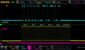
Figure 1: Basic SPI Analysis with analogue oscilloscope channels
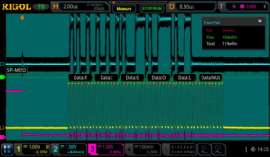
Figure 2: Pass / Fail Analysis to highlight crosstalk on a communication bus
One advantage to this approach is that masks can easily be saved and reused on different board revisions or code revisions within a project. Simple tests can therefore help to quickly identify the version or build that first showed an increase in noise or change in performance. It is important to internalise that the opposite can be true as well. Device performance may be so reliable that different layouts or smaller wires for connections may be possible creating more freedom for the overall mechanical design.
When there are issues with bandwidth or signal levels impedance may ultimately be the culprit. High impedance probing is made to deliver maximum voltage to the scope, but many serial buses have characteristic impedance such as 50 Ohms. In these cases, a valuable test is to transmit signals directly into a 50 Ohm probe setting on the oscilloscope. This makes it possible to visualise what the 50 Ohm receiving end sees during a transmission. If the impedance of the cabling, connections, or transmitter is off then the amplitude may droop or square waves may be misshapen. Regardless of the impedance of your lines, there are RC components that affect the risetime and overshoot of the transitions. Selecting the wrong termination resistors for your bus can cause extraneous power drain or poor transmission settling. System bandwidth and line impedance issues can be caused by these resistances as well as excessive or unstable capacitance. Like noise, these symptoms usually indicate physical hardware issues beyond basic valid data transmissions. When significant data errors or bugs do come into play another verification method can be used. To get a clearer image of how our IoT platform is interpreting this data we can use our mixed signal channels for comparison.
The digital channels on the oscilloscope (shown on the bottom of Figure 3) can be set with threshold values that mimic the bus controller on the IoT platform.
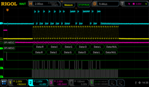
Figure 3: Comparison with mixed signal channels for data interpretation
The device does not see the analogue signals, but interprets their digital equivalent. Therefore, when having data issues it is important to look at both the digital and analogue representation. This enables engineers to quickly discover where data failures are occurring as well as the analogue root cause or noise source that may be contributing.
Lastly, one important consideration when implementing sensors in an IoT device is the latency between bus communication and action. Of course, this is highly dependent on both the platform and the code methodology and can change dramatically. Latency is the time it takes for the system or platform to interpret the peripheral data and take an action. As a latency baseline we ran a simple test that toggles an LED when a SPI read is completed. The cursor measurements on Figure 4 highlight this.
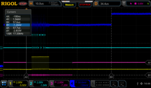
Figure 4: Latency measurement from SPI bus to LED on our IoT development board
From this baseline on your platform you can model how code changes impacts this latency and then you can base decisions about servicing these sensors based on the balance of use case and reliability requirements with battery life and implementation.
Latency, noise, bandwidth, and impedance all effect signal integrity and reliability. These key measurement techniques can be used throughout development, use case, and reliability testing to optimise the overall design and anticipate failure modes. As part of an overall IoT design strategy, continuous evaluation of signal integrity established baselines and limits helps speed time to market and customer acceptance with small impact to equipment budgets.
Conclusions and Key Learnings
When working in the fast changing atmosphere of IoT design and development reliable test methodologies become increasingly important. As engineers integrate the newest sensors and platforms on the fly to reach highly competitive markets as fast as possible, understanding core customer requirements and trade-offs and how those can be evaluated and compared throughout the development is an important step toward improving the strategic design process.
Whether the challenges of an application are more form or function, issues related to signal integrity and reliability are fundamental elements of design in the IoT ecosystem that play a significant role in market success. Establishing these principles early in the process and testing them iteratively is one of the best ways to limit budget and schedule risks in the latter stages of the design. Modern, easy to use test equipment that is more affordable than ever can be utilised to develop the limits and baselines that will guide an engineering team through a successful product development.
Products Mentioned In This Article:
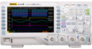
- DS1000Z Series please see HERE